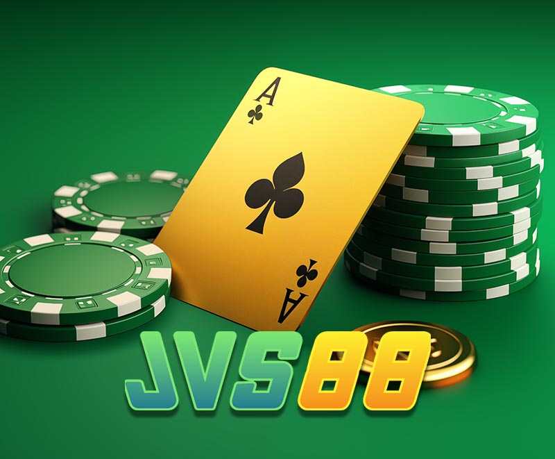
Home

Home

About Us

The Team
History

Industry Info

Industry Calender
Industry News
Industry Links
Recruitment
Business Opportunities

Technology

Nanotechnology
MEMs
Semiconductors
Solar
Plastic Electronics

Membership

Membership list
Membership Benefits
join Now

JEMI Media

Press Releases
Exhibitions
Newsletter

Technical Visits

Calender
Photo Library

Contact Us

Contact Form

Member Login


MEMBERSHIP LIST

      Date :  
Site Search:

Sitemap
 
Company Name Product or Service Company Logo (Hyperlink)

Alcatel Vacuum Technology
(U.K.) Ltd

Alcatel Vacuum Technology has launched Adixen, its new brand name, in recognition of the company's international standing in vacuum technology. With 40 years of experience, Alcatel Vacuum Technology today has a worldwide presence and world-class products. With both ISO 9001 and 14001 certification, Alcatel Vacuum Technology is an acknowledged expert in service and support, and Adixen products have the highest quality and environmental standards. Alcatel Vacuum Technology will remain as an important part of the Alcatel group with its complete power for innovations and development and the security that can only be offered by a group such as Alcatel.

adixen
BFi Optilas

We represent many leading suppliers that offer products that cover the following product areas: Imaging & Detection, Lasers & Accessories, Optical Components, RF Microwave & Fibre Optics, Test & Measurment and Interconnect, Passive & Electromechanical Components

bfioptilas.co.uk

Bronkhorst (UK) Ltd

Bronkhorst, as European market leaders, manufacture the widest range of Thermal and Coriolis Mass Flow Meters/Controllers for gases and liquids, Electronic Pressure Controllers and Vapour Generation Systems available on the market. Recent innovations include ultra fast response and user selectable multi-gas/multi-range capability. Gas flow control ranges from 0.02 mln/min to 11,000 m3/hr whilst liquid control ranges from 25 nanolitres/min to 600 kg/hr. Pressure control ranges from vacuum to 700 bar. Standard UHP designs are complimented by Laboratory, Industrial and ATEX Approved configurations. Bronkhorst offers world-wide local sales and after-sales support, calibration and service facilities, application engineering and user training courses.

bronkhorst

Cambridge Nanotech Inc.

As the leading provider of Atomic Layer Deposition (ALD) solutions, Cambridge NanoTech has over 175 ALD systems installed worldwide. Cambridge NanoTech applies its expertise to solve unique coating challenges by collaborating on breakthrough research with customers and by offering next-generation thermal, plasma-enhanced and large-area ALD systems. To learn more, please visit us at www.cambridgenanotech.com.

cnt

CCLRC

The CCLRC is one of Europe's largest multidisciplinary research organisations supporting scientists and engineers world-wide.

CCLRC

CEI-Europe AB

The mission of CEI Europe is to provide the International community of scientists and engineers with education in advanced technologies. Over the years, Dr Birgit E Jacobson, founder and CEO, has received the recognition of her peers as scientist and educationalist. Most recently was made Honorary By-Fellow of Churchill College at the University of Cambridge, England 2001, and Honorary Doctor at Chalmers Institute of Technology, Sweden 2003.


CEI

CH2M Hill

CH2M HILL is a large design and project management company, which specialises in facility solutions for the electronics industry. Our scope of services includes concept and feasibility studies, planning, design, project management, energy consulting, turnkey design and construction, cleanroom construction and industrial engineering.  We have been responsible for the design and construction of some of the World’s leading facilities. Our global experience enables us to benchmark our clients’ projects.  From our base in Glasgow, we provide deliver projects throughout the UK and Europe. Contact Ian Tonge – 07753 771498


C2Mhill

Compugraphics International Ltd

Shaping total, global photomask solutions. Compugraphics has for over 40 years provided technical and service excellence, supplying integrated photomask solutions to the global semiconductor, microelectronics and optoelectronics industry from our manufacturing facilities in Glenrothes, Scotland (certified to QS9000TE & ISO14001 standard) and Los Gatos, California, USA. Our reticle repair and recertification site located in Austin, Texas, provides complementary repell services.


Compugraphics

DuPont de Nemours S.A.

DuPont™ Kalrez® Perfluoroelastomer Parts and DuPont™ Vespel® Parts For Aggressive Semiconductor Environments
Kalrez® perfluoroelastomer parts have been field-proven in the manufacture of semiconductors where extremes of thermal and chemical exposure are involved and purity is critical to high semiconductor wafer yield.  Using Kalrez® parts reduces the risk of contamination from particulates, outgassing and extractables caused by seal deterioration. Very broad chemical resistance coupled with superior high-temperature properties enables Kalrez® parts to withstand virtually any process media, including plasma with various gases at temperatures up to 325°C.

Processors can improve semiconductor seal performance in all wafer-fabricating operations, including thermal, deposition, etching, ashing/stripping, and wet chemical processes.   Users of Kalrez® have the assurance of quality and traceability of all parts made at the company's ISO 9001/9002 and AS 9100-registered facilities in the U.S. and Japan. No other high performance seal manufacturer offers this total control over product quality and end-use applications.

DuPont™ Vespel® parts and shapes reduce ownership costs with longer life in the chamber and extended maintenance intervals. And they often cost less right up front. DuPont™ Vespel® parts and shapes come with a documented record of reliability and durability in wafer handling, wafer processing, IC handling and testing and other semiconductor manufacturing operations.  The particular wear performance and ultra clean nature of the polymer allows longer life time of wafer contact parts and contamination free operation processes in the Etching area.  Vespel® offers a number of great chemical resistance materials that allow excellent wear performance to the retaining ring solutions, providing customers with longer part life and remarkable cost of ownership reduction.  For wafer handling and end effectors, the non scratching, ultra low wear performance has made DuPont™ Vespel® a favorite choice of wafer contact material. With newly developed conductive grade, Vespel® offers great solutions to ESD change reduction. Also, a ultra high modulus composite product line offers low deflection wafer handling effectors with vibration damping effect.


Ebara Precision Machinery

EBARA provides high quality products and solutions for vacuum generation + waste gas treatment as well as state-of-the-art wafer processing tools. Our primary markets are semiconductor, photovoltaics and sophisticated vacuum applications. Our primary markets are semiconductor, photovoltaics and sophisticated vacuum applications.

ebara

IDB Technologies Ltd

Wafers, Automation, optical microscopy and second user systems.

IDB

Innodys

A European Semiconductor Systems and Components Distribution Organisation

innodys

IQE

IQE is the Global Leader in Wafer Outsourcing. The company is the world leading merchant epiwafer supplier for the compound semiconductor industry and has 6 manufacturing sites worldwide in Europe, USA and the Far East.

IQE

James Walker Ltd

We work constantly at the forefront of fluid seal development and materials science to provide industries worldwide with the top-quality products that are vital to the safe and efficient operation of plant and machinery. We are a UK-based company with a global reputation for solving fluid sealing problems. We bring practical expertise and leading edge technology to the custom-design of optimum sealing solutions to match our customers' exact operational specifications — backed by testing and manufacturing to world-class standards.


JLS Designs

The Company was formed to provide design and manufacturing services to the R&D Semiconductor Industry. Since our formation we have been involved with several turn key projects and have developed a complete range of processing equipments. Our unique approach and abilities enable us to provide solutions tailored to our customers requirements.


JLS

Kratos Analytical Ltd

The Shimadzu series of wide-range Magnetically Levitated Turbo Molecular Pumps, with capacities from 200L/s to 4200L/s for Etch, Implant and PVD/CVD process and high compression sputtering applications. 'Nova' fully automated 200mm wafer capability, high speed parallel imaging & small spot electron spectrometer (ESCA-XPS), and 'AXIS-ULTRA'; high speed parallel imaging & small spot electron spectrometer (ESCA-XPS).

www.kratos.co.uk

Laurell Technologies Corporation

Laurell’s at the forefront of practical/affordable tool design yet dedicated to customer satisfaction. We have systems installed worldwide and an excellent reputation for doing what we say ... since 1985! Our UK service/support centre assists our UK/European customers with all technical/processing issues, servicing/repairs, training, and spares. • Lifetime process development support from US/UK • Application-specific approach offers more functionality at less cost • All universally-designed systems are configured to meet YOUR needs. • We’re experts at handling substrates; designing chucks, then manufacturing them from the finest materials available • We typically repair most equipment in <24 hours • Laurell systems are easy to use, and sophisticated in design. The user can develop a process for their application, while maintaining safe visualization of their substrate. If you need to apply a thin coating to a substrate, then develop and/or etch it, then we have the right tool at the right price.

Welcome to Laurell Technologies Corporation!  Home of fine spin coating, spin etching, spin developing and other semiconductor equipment

Metryx

Metryx has developed a unique mass metrology technology for semiconductor manufacturers. Today the technology is in volume production 200mm and 300mm fabs all over the world. It is helping to ramp production wafers quicker than at any other time before and is also helping fabs running at capacity to make sure their process is running optimally. This innovative metrology utilises the simplest of measurement parameters and the very basics of physics – everything has a mass and undergoes mass change during process. Characterizing a wafer’s mass with atomic precision can non-destructively and non-intrusively highlight process problems quicker than any other form of metrology. It does this on actual product wafers and at a fraction of the cost of existing metrology solutions.

metryx
MKS Instruments
MKS Instruments Inc. is a leading worldwide provider of process control solutions for advanced manufacturing processes such as semiconductor device manufacturing, thin-film manufacturing for flat panel displays, optical storage media, architectural glass and electro-optical products and technology for medical equipment.
mks

Nanotechnology KTN

The mission of the Nanotechnology Knowledge Transfer Network (NanoKTN) is to encourage and support organisations to collaborate and share knowledge with key partners in attractive end user markets to achieve growth of the UK nanotechnology sector.

NOR-CAL Ltd

Manufacturers of high vacuum & UHV components for semiconductor, research,  thin film deposition and other applications for 36 years.

No-cal logo.gif (1030 bytes)

Oerlikon Leybold Vacuum (UK) Ltd

Oerlikon Leybold Vacuum offers a wide range of advanced vacuum solutions for use in manufacturing and analytical processes, as well as for research purposes. Using the experience of 156 years in vacuum technology, Oerlikon Leybold Vacuum offers a broad know how of processes and applications to their customers, supported by the largest world wide sales and after sales network. Oerlikon Leybold Vacuum ranks among the top three providers in its specific business segments, which are Process Industry, Information Technology, Analytical Processes and Research & Development.

oerlikon

OM Group Ultra Pure Chemicals

YOUR GLOBAL PARTNER FOR QUALITY PRODUCTS AND SERVICES

Acids, Solvents, Bases and Bespoke Mixtures are produced and supplied to the semiconductor industry by OM Group Ultra Pure Chemicals. We provide world class quality and service guarantees supported by many years of experience in the manufacture and supply of high quality Ultra Pure Chemicals for Cleaning, Etching and Stripping processes, plus Photolithography products.

OM Group Ultra Pure Chemicals produce and supply a wide range of chemicals all manufactured to strict product specifications to meet your requirements. Precise concentration control High Purity Chemicals with low cation/anion levels (to <0.1ppb) and filtered products Total Chemical Management Services Bespoke Solutions Statistical Process Controlled Manufacturing Quality Assurance - ISO9000, TS16949, ISO17025 Health, Safety & Environment - ISO14001, OHSAS18001, IPPC, COMAH registered sites Analytical Services - Cation analysis, particle counts, assay determination of process chemicals

omg group

Oxford Instruments Plasma
Technology Ltd

Oxford Instruments offers flexible, configurable process tools and leading-edge processes for the precise, controllable and repeatable etching, deposition and growth of micro- and nano-structures. Our systems provide process solutions for the micro- and nanometre engineering of materials for semiconductor, optoelectronics, MEMS & microfluidics, high quality optical coating and many other applications in micro- and nanotechnology.

These solutions are based on core technologies in:

- Plasma Etch & Deposition
- Atomic Layer Deposition (ALD)
- Ion Beam Etch & Deposition
- Nanoscale Growth Systems
- Hydride Vapour Phase Epitaxy (HVPE)

Products range from compact stand-alone systems for R&D, through to batch tools and up to cassette-to-cassette and clustered platforms for production processing.

OXFORD

Pall Corporation

Filtration and separation technology

Pall
Plasma-Therm Plasma-Therm LLC is the global technological leader for providing thin film etch and plasma deposition equipment to a number of high tech market segments and industries. These customer focused solutions are used in areas ranging from university R&D to high volume production.
plasma

SAFC Hitech

SAFC Hitech provides a unique chemistry service translating application understanding into performance materials worldwide. Through collaborative partnerships and an integrated approach from research and development, process development and scale up to commercial manufacturing, SAFC Hitech invests in innovation and manufacturing enabling current and future technology needs.

Welcome to SAFC Hitech

Saint-Gobain Semicon Services Ltd

Component cleaning and refurbishment services.


Scottish Microelectronics Centre

The Scottish Microelectronics Centre is Scotland’s world class centre for Incubation, Analysis and Research and Development in the semiconductor sector. Our key strengths are in-house analytical imaging and repair facilities, microfabrication and MEMS processing, specialist business and technology incubation and low volume rapid turnaround packaging solutions.

smc

Silson Ltd

Standard silicon nitride membrane windows.

silson

Sistem Technology

Sistem Technology offers a product portfolio second to none for Semiconductor and Advanced Technology R & D, Production and OEM applications. Wet Process: Batch and single substrate processing, including spin coating, develop, bake, lift-off, etch and clean. Chemical distribution systems, megasonics, DI water/chemical in-line and immersion heaters, gas and solvent heaters. Thermal Processing: Horizontal and vertical furnaces. Advanced controllers, replacement elements and vestibule blocks for most furnace types. Also ovens, quartzware and high capacity vacuum traps. Photolithography: R&D and Production contact, proximity and projection mask aligners. Reticle storage systems. Films: Atomic Layer Deposition (ALD) tools for research and production Test: Epoxy/Blade probe cards including ultra low leakage. Probe cleaning materials. Automation: Assembly, integration, retrofit and servicing of E.F.E.Ms, A.M.H.S and related S.M.I.F modules. Automated wafer/cassette transfer systems. RFID and IR read/write systems. BCR/OCR readers. Complete interface solutions.


sistem

Southampton Nanofabrication Centre

The Southampton Nanofabrication Centre  (SNC) is a new clean-room facility dedicated to the fabrication and patterning of materials at the nanoscale for both Academic and Industrial users.  At the heart of the new facility is a JEOL 9300 FS direct write electron beam lithography system specified with a 20nm line width writing capability but practically exhibiting 10nm resolution.  In addition, the SNC houses a fully-comprehensive range of nanofabrication and optical/electrical characterisation equipment.  Beyond a suite of optical and electron microscopes a range of deposition systems are a available and a fully-equipped wet-room and full electrical characterisation facilities are also housed within the SNC.


snc

SPS (UK) Ltd

SPS is a full-service distributor to the semiconductor and associated
industries. We supply a complete range of Wafer Handling tools, from Vacuum Wands, Aligners, Transfers, Sorters and Inspection tools, to wafer Cassettes, Storage boxes and wafer Packing and Shipping products. We also supply Spin Coaters, Mask Aligners, Nano-Imprint modules, Megasonic Generators, and a full range of DI & Chemical Heaters, Flow-meters, Pumps, Tanks, Valves and Fittings, as well as a range of consumables for CMP.

sps

SPP Process Technology Systems Limited

Formed following the merger of Aviza Technology and Surface Technology Systems, SPP Process Technology Systems Limited (SPTS) is a supplier of cassette to cassette cluster and single/batch loadlocked plasma etch and deposition systems that can be configured with ICP, XeF2, PVD, MOCVD and PECVD sources. Products include the market-leading ASE® deep silicon etch process for MEMS micromachining and 3D-IC packaging, plus plasma processes for metals, polymers, dielectrics and compound semiconductors.

Surface Technology Systems Homepage


University of Edinburgh

Microelectronics research

www.ee.ed.ac.uk

Veonis Technologies Ltd

Supplier of metrology equipment and systems for wafer handling and automation.

veonis


West European Semiconductor Technology Ltd

European Supplier of: *Gas purifiers* # *Rapid Thermal Processors*
# *Furnaces, from bench top to production* # *Furnace elements* # *Quartzware* # *Mass Flow Controllers & Meters (digital & analogue)* # *Liquid & Vapour Flow Controllers* # *Bellows & Diaphragm Valves* # *GaAs & other compound semiconductor wafers* # *Gallium source material*

west assoc

Watlow Ltd

Since the company's founding in 1922, Watlow has brought its thermal expertise to numerous applications, including semiconductor, photovoltaic, analytical, medical, clinical, plastics processing, foodservice equipment, packaging, aerospace and others.  Headquartered in St. Louis, Missouri, Watlow is the largest custom designer and manufacturer of industrial heaters, sensors, controllers and software with offices and manufacturing facilities around the world.

watlow


collaboration vdma sssf jemi france semi

JEMI UK Ltd, The King's Buildings, West Mains Road, Edinburgh EH9 3JF  Tel: + 44 (0) 131 650 7815 E-mail: jemi-enquiries@see.ed.ac.uk

© www.jemiuk.com 2008